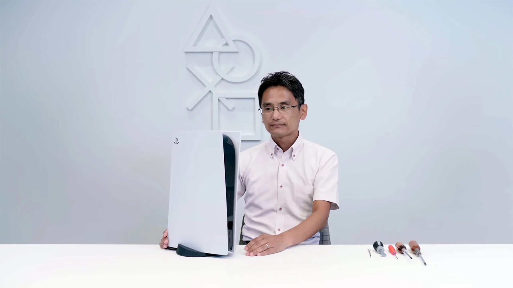
PS5 teardown

Yasuhiro Ootori. © Sony Interactive Entertainment.
It seems that Sony beat iFixit to the punch by making their own teardown video of its PlayStation 5 console, long before its launch, scheduled for November 12. In the video, in Japanese with English sub-titles, Yasuhiro Ootori, VP of mechanical design at Sony Interactive Entertainment, thoroughly and painstakingly dismantles the new console. The video reveals much about the design of the machine, especially the engineering pains taken to ensure proper cooling. We learned, among other things, that Sony uses a liquid metal thermal conductor on the surface of the AMD RyZen SoC instead of the usual heat paste in order to optimize heat transfer to a huge dissipator. The entire system seems easy to take apart with a few standard screwdrivers. Even so, we’ll have to wait for iFixit’s teardown to get a repairability score. Kyle Wiens, iFixit’s CEO, said in an email to Motherboard, “This level of transparency from a manufacturer is refreshing”. Indeed, electronics manufacturers providing instructions on how to take their products apart is as rare as an oasis in a desert.
⇨ YouTube, “PS5 Teardown: An up-close and personal look at the console hardware.”
⇨ Ars Technica, Kyle Orland, “The first PlayStation 5 teardown reveals some hardware secrets.”
