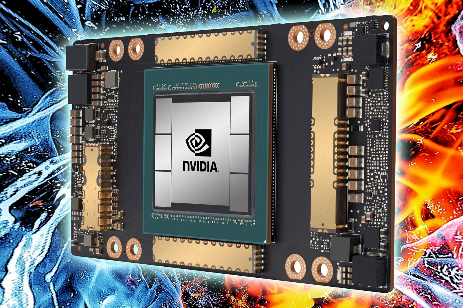
Nvidia DGX A100

A100. © Nvidia.
Nvidia is unveiling its next-generation Ampere GPU architecture today. The first GPU to use Ampere will be Nvidia’s new A100, built for scientific computing, cloud graphics, and data analytics. While there have been plenty of rumors around Nvidia’s Ampere plans for GeForce “RTX 3080” cards, the A100 will primarily be used in data centers. The DGX A100 system promises 5 petaflops of performance and various other exceptional features, but all of this performance isn’t going into powering the latest version of Assassin’s Creed (?)… The A100 sports more than 54 billion transistors, making it the world’s largest 7nm processor. “That is basically at nearly the theoretical limits of what’s possible in semiconductor manufacturing today,” explains Nvidia CEO Jensen Huang. “The largest die the world’s ever made, and the largest number of transistors in a compute engine the world’s ever made.” Systems start at USD199,000, which made it an expensive game of Assassin’s Creed anyway.
⇨ YouTube, “Introducing NVIDIA DGX A100.”
⇨ The Verge, Tom Warren, James Vincent, “Nvidia’s first Ampere GPU is designed for data centers and AI, not your PC.”
